
74HC109-Q100; 74HCT109-Q100
Dual JK flip-flop with set and reset; positive-edge-trigger
The 74HC109?-?Q100; 74HCT109?-?Q100 is a dual positive edge triggered JK flip?-?flop featuring individual J and K inputs, clock (CP) inputs, set (SD) and reset (RD) inputs and complementary Q and Q outputs. The set and reset are asynchronous active LOW inputs and operate independently of the clock input. The J and K inputs control the state changes of the flip?-?flops as described in the mode select function table. The J and K inputs must be stable one set?-?up time prior to the LOW?-?to?-?HIGH clock transition for predictable operation. The JK design allows operation as a D?-?type flip?-?flop by connecting the J and K inputs together. This device features reduced input threshold levels to allow interfacing to TTL logic levels. Inputs also include clamp diodes, this enables the use of current limiting resistors to interface inputs to voltages in excess of VCC.
Schmitt?-?trigger action in the clock input makes the circuit highly tolerant to slower clock rise and fall times.
This product has been qualified to the Automotive Electronics Council (AEC) standard Q100 (Grade 1) and is suitable for use in automotive applications.
Features and benefits
Automotive product qualification in accordance with AEC-Q100 (Grade 1)
Specified from -40 °C to +85 °C and from -40 °C to +125 °C
J and K inputs for easy D-type flip-flop
Toggle flip-flop or "do nothing" mode
Wide supply voltage range:
For 74HC109-Q100: from 2.0 V to 6.0 V
For 74HCT109-Q100: from 4.5 V to 5.5 V
CMOS low power dissipation
High noise immunity
Input levels:
For 74HC109-Q100: CMOS level
For 74HCT109-Q100: TTL level
Latch-up performance exceeds 100 mA per JESD 78 Class II Level B
74HC109-Q100 complies with JEDEC standards:
JESD8C (2.7 V to 3.6 V)
JESD7A (2.0 V to 6.0 V)
74HCT109-Q100 complies with JEDEC standard JESD7A (2.0 V to 6.0 V)
ESD protection:
HBM: ANSI/ESDA/JEDEC JS-001 class 2 exceeds 2000 V
CDM: ANSI/ESDA/JEDEC JS-002 class C3 exceeds 1000 V
參數(shù)類型
| 型號 | VCC (V) | Logic switching levels | Output drive capability (mA) | tpd (ns) | fmax (MHz) | Power dissipation considerations | Tamb (°C) | Rth(j-a) (K/W) | Ψth(j-top) (K/W) | Rth(j-c) (K/W) | Package name |
|---|---|---|---|---|---|---|---|---|---|---|---|
| 74HC109D-Q100 | 2.0?-?6.0 | CMOS | ± 5.2 | 15 | 75 | low | -40~125 | 86 | 6.6 | 44 | SO16 |
| 74HCT109D-Q100 | 4.5?-?5.5 | TTL | ± 4 | 17 | 61 | low | -40~125 | 86 | 6.6 | 44 | SO16 |
| 74HCT109PW-Q100 | 4.5?-?5.5 | TTL | ± 4 | 17 | 61 | low | -40~125 | 119 | 3.2 | 48.1 | TSSOP16 |
封裝
| 型號 | 可訂購的器件編號,(訂購碼(12NC)) | 狀態(tài) | 標示 | 封裝 | 外形圖 | 回流焊/波峰焊 | 包裝 |
|---|---|---|---|---|---|---|---|
| 74HC109D-Q100 | 74HC109D-Q100J (935334221118) |
Active | 74HC109D |
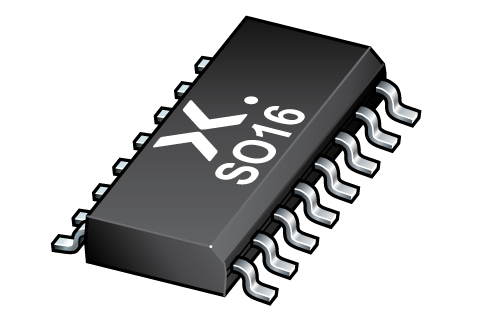
SO16 (SOT109-1) |
SOT109-1 |
SO-SOJ-REFLOW
SO-SOJ-WAVE WAVE_BG-BD-1 |
SOT109-1_118 |
| 74HCT109D-Q100 | 74HCT109D-Q100J (935332777118) |
Active | 74HCT109D |
SO16 (SOT109-1) |
SOT109-1 |
SO-SOJ-REFLOW
SO-SOJ-WAVE WAVE_BG-BD-1 |
SOT109-1_118 |
| 74HCT109PW-Q100 | 74HCT109PW-Q100J (935336488118) |
Active | HCT109 |
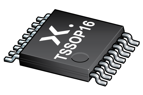
TSSOP16 (SOT403-1) |
SOT403-1 |
SSOP-TSSOP-VSO-WAVE
|
SOT403-1_118 |
環(huán)境信息
| 型號 | 可訂購的器件編號 | 化學成分 | RoHS | RHF指示符 |
|---|---|---|---|---|
| 74HC109D-Q100 | 74HC109D-Q100J | 74HC109D-Q100 |
|
|
| 74HCT109D-Q100 | 74HCT109D-Q100J | 74HCT109D-Q100 |
|
|
| 74HCT109PW-Q100 | 74HCT109PW-Q100J | 74HCT109PW-Q100 |
|
|
文檔 (15)
| 文件名稱 | 標題 | 類型 | 日期 |
|---|---|---|---|
| 74HC_HCT109_Q100 | Dual JK flip-flop with set and reset; positive-edge-trigger | Data sheet | 2024-02-21 |
| AN11044 | Pin FMEA 74HC/74HCT family | Application note | 2019-01-09 |
| AN90063 | Questions about package outline drawings | Application note | 2025-06-13 |
| SOT109-1 | 3D model for products with SOT109-1 package | Design support | 2020-01-22 |
| SOT403-1 | 3D model for products with SOT403-1 package | Design support | 2020-01-22 |
| Nexperia_package_poster | Nexperia package poster | Leaflet | 2020-05-15 |
| SO16_SOT109-1_mk | plastic, small outline package; 16 leads; 1.27 mm pitch; 9.9 mm x 3.9 mm x 1.35 mm body | Marcom graphics | 2017-01-28 |
| TSSOP16_SOT403-1_mk | plastic, thin shrink small outline package; 16 leads; 0.65 mm pitch; 5 mm x 4.4 mm x 1.1 mm body | Marcom graphics | 2017-01-28 |
| SOT109-1 | plastic, small outline package; 16 leads; 1.27 mm pitch; 9.9 mm x 3.9 mm x 1.75 mm body | Package information | 2023-11-07 |
| SOT403-1 | plastic, thin shrink small outline package; 16 leads; 5 mm x 4.4 mm x 1.2 mm body | Package information | 2023-11-08 |
| SO-SOJ-REFLOW | Footprint for reflow soldering | Reflow soldering | 2009-10-08 |
| HCT_USER_GUIDE | HC/T User Guide | User manual | 1997-10-31 |
| SO-SOJ-WAVE | Footprint for wave soldering | Wave soldering | 2009-10-08 |
| WAVE_BG-BD-1 | Wave soldering profile | Wave soldering | 2021-09-08 |
| SSOP-TSSOP-VSO-WAVE | Footprint for wave soldering | Wave soldering | 2009-10-08 |
支持
如果您需要設(shè)計/技術(shù)支持,請告知我們并填寫 應答表 我們會盡快回復您。
Ordering, pricing & availability
樣品
作為 Nexperia 的客戶,您可以通過我們的銷售機構(gòu)訂購樣品。
如果您沒有 Nexperia 的直接賬戶,我們的全球和地區(qū)分銷商網(wǎng)絡可為您提供 Nexperia 樣品支持。查看官方經(jīng)銷商列表。