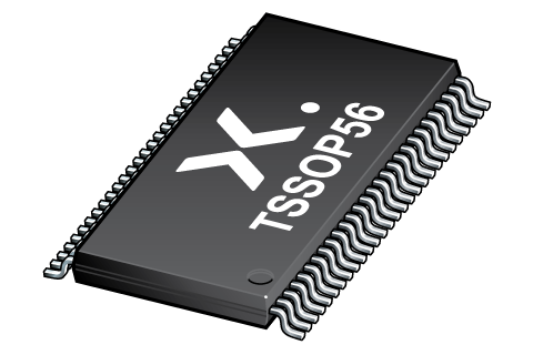
74LVT16500A
3.3 V 18-bit universal bus transceiver; 3-state
The 74LVT16500A is a high-performance BiCMOS product designed for VCC operation at 3.3 V.
This device is an 18-bit universal transceiver featuring non-inverting 3-state bus compatible outputs in both send and receive directions. Data flow in each direction is controlled by output enable (OEAB and OEBA), latch enable (LEAB and LEBA), and clock (CPAB and CPBA) inputs. For A-to-B data flow, the device operates in the transparent mode when LEAB is HIGH. When LEAB is LOW, the A data is latched if CPAB is held at a HIGH or LOW logic level. If LEAB is LOW, the A-bus data is stored in the latch/flip-flop on the HIGH-to-LOW transition of CPAB. When OEAB is HIGH, the outputs are active. When OEAB is LOW, the outputs are in the high-impedance state.
Data flow for B-to-A is similar to that of A-to-B but uses OEBA, LEBA and CPBA. The output enables are complimentary (OEAB is active HIGH, and OEBA is active LOW).
Active bus-hold circuitry is provided to hold unused or floating data inputs at a valid logic level.
Features and benefits
- 18-bit bidirectional bus interface
- 3-state buffers
- Output capability: +64 mA and -32 mA
- TTL input and output switching levels
- Input and output interface capability to systems at 5 V supply
- Bus-hold data inputs eliminate the need for external pull-up resistors to hold unused inputs
- Live insertion/extraction permitted
- Power-up reset
- Power-up 3-state
- No bus current loading when output is tied to 5 V bus
- Negative edge-triggered clock inputs
- Latch-up protection:
- JESD78: exceeds 500 mA
- ESD protection:
- MIL STD 883 Method 3015: exceeds 2000 V
- CDM JESD22-C101-C exceeds 1000 V
Applications
參數類型
| 型號 |
|---|
封裝
下表中的所有產品型號均已停產 。
| 型號 | 可訂購的器件編號,(訂購碼(12NC)) | 狀態 | 標示 | 封裝 | 外形圖 | 回流焊/波峰焊 | 包裝 |
|---|---|---|---|---|---|---|---|
| 74LVT16500ADGG | 74LVT16500ADGG,112 (935203020112) |
Obsolete | LVT16500A Standard Procedure Standard Procedure |

TSSOP56 (SOT364-1) |
SOT364-1 |
SSOP-TSSOP-VSO-WAVE
|
暫無信息 |
| 74LVT16500ADGG,118 (935203020118) |
Obsolete | LVT16500A Standard Procedure Standard Procedure | SOT364-1_118 | ||||
| 74LVT16500ADGGS (935203020512) |
Obsolete | LVT16500A Standard Procedure Standard Procedure | 暫無信息 | ||||
| 74LVT16500ADGGY (935203020518) |
Obsolete | LVT16500A Standard Procedure Standard Procedure | 暫無信息 |
環境信息
下表中的所有產品型號均已停產 。
| 型號 | 可訂購的器件編號 | 化學成分 | RoHS | RHF指示符 |
|---|---|---|---|---|
| 74LVT16500ADGG | 74LVT16500ADGG,112 | 74LVT16500ADGG |
|
|
| 74LVT16500ADGG | 74LVT16500ADGG,118 | 74LVT16500ADGG |
|
|
| 74LVT16500ADGG | 74LVT16500ADGGS | 74LVT16500ADGG |
|
|
| 74LVT16500ADGG | 74LVT16500ADGGY | 74LVT16500ADGG |
|
|
文檔 (12)
| 文件名稱 | 標題 | 類型 | 日期 |
|---|---|---|---|
| 74LVT16500A | 3.3 V 18-bit universal bus transceiver; 3-state | Data sheet | 2006-05-28 |
| AN90063 | Questions about package outline drawings | Application note | 2025-06-13 |
| 001aaf035 | Block diagram: 74LVT16500ADGG, 74LVT16500ADL | Block diagram | 2009-11-04 |
| 001aaf038 | Block diagram: 74LVT16500ADGG, 74LVT16500ADL | Block diagram | 2009-11-04 |
| 001aaf039 | Block diagram: 74LVT16500ADGG, 74LVT16500ADL | Block diagram | 2009-11-04 |
| 001aaf040 | Block diagram: 74LVT16500ADGG, 74LVT16500ADL | Block diagram | 2009-11-04 |
| SOT364-1 | 3D model for products with SOT364-1 package | Design support | 2020-01-22 |
| lvt16500a | lvt16500a IBIS model | IBIS model | 2013-04-09 |
| Nexperia_package_poster | Nexperia package poster | Leaflet | 2020-05-15 |
| SOT364-1 | plastic, thin shrink small outline package; 56 leads; 0.5 mm pitch; 14 mm x 6.1 mm x 1.2 mm body | Package information | 2022-06-23 |
| lvt16 | lvt16 Spice model | SPICE model | 2013-05-07 |
| SSOP-TSSOP-VSO-WAVE | Footprint for wave soldering | Wave soldering | 2009-10-08 |
支持
如果您需要設計/技術支持,請告知我們并填寫 應答表 我們會盡快回復您。
Ordering, pricing & availability
樣品
作為 Nexperia 的客戶,您可以通過我們的銷售機構訂購樣品。
如果您沒有 Nexperia 的直接賬戶,我們的全球和地區分銷商網絡可為您提供 Nexperia 樣品支持。查看官方經銷商列表。