
74LVC8T245-Q100; 74LVCH8T245-Q100
8-bit dual supply translating transceiver; 3-state
The 74LVC8T245-Q100; 74LVCH8T245-Q100 are 8-bit dual supply translating transceivers with 3-state outputs that enable bidirectional level translation. They feature two data input-output ports (pins An and Bn), a direction control input (DIR), an output enable input (OE) and dual supply pins (VCC(A) and VCC(B)). Both VCC(A) and VCC(B) can be supplied at any voltage between 1.2 V and 5.5 V. This flexibility makes the device suitable for translating between any of the low voltage nodes (1.2 V, 1.5 V, 1.8 V, 2.5 V, 3.3 V and 5.0 V). Pins An, OE and DIR are referenced to VCC(A) and pins Bn are referenced to VCC(B). A HIGH on DIR allows transmission from An to Bn and a LOW on DIR allows transmission from Bn to An. The output enable input (OE) can be used to disable the outputs so the buses are effectively isolated.
The devices are fully specified for partial power-down applications using IOFF. The IOFF circuitry disables the output, preventing any damaging backflow current through the device when it is powered down. In suspend mode when either VCC(A) or VCC(B) are at GND level, both A port and B port are in the high-impedance OFF-state.
Active bus hold circuitry in the 74LVCH8T245-Q100 holds unused or floating data inputs at a valid logic level.
This product has been qualified to the Automotive Electronics Council (AEC) standard Q100 (Grade 1) and is suitable for use in automotive applications.
Features and benefits
Automotive product qualification in accordance with AEC-Q100 (Grade 1)
Specified from -40 °C to +85 °C and from -40 °C to +125 °C
Wide supply voltage range:
VCC(A): 1.2 V to 5.5 V
VCC(B): 1.2 V to 5.5 V
High noise immunity
Complies with JEDEC standards:
JESD8-7 (1.2 V to 1.95 V)
JESD8-5 (1.8 V to 2.7 V)
JESD8C (2.7 V to 3.6 V)
JESD36 (4.5 V to 5.5 V)
Maximum data rates:
420 Mbps (3.3 V to 5.0 V translation)
210 Mbps (translate to 3.3 V))
140 Mbps (translate to 2.5 V)
75 Mbps (translate to 1.8 V)
60 Mbps (translate to 1.5 V)
Suspend mode
Latch-up performance exceeds 100 mA per JESD 78B Class II
±24 mA output drive (VCC = 3.0 V)
Inputs accept voltages up to 5.5 V
Low power consumption: 30 μA maximum ICC
IOFF circuitry provides partial Power-down mode operation
ESD protection:
HBM: ANSI/ESDA/JEDEC JS-001 class 3A exceeds 4000 V
CDM: ANSI/ESDA/JEDEC JS-002 class C3 exceeds 1000 V
DHVQFN package with Side-Wettable Flanks enabling Automatic Optical Inspection (AOI) of solder joints
參數類型
| 型號 | VCC(A) (V) | VCC(B) (V) | Logic switching levels | Output drive capability (mA) | tpd (ns) | Nr of bits | Power dissipation considerations | Tamb (°C) | Rth(j-a) (K/W) | Ψth(j-top) (K/W) | Rth(j-c) (K/W) | Package name | Category |
|---|---|---|---|---|---|---|---|---|---|---|---|---|---|
| 74LVC8T245BQ-Q100 | 1.2?-?5.5 | 1.2?-?5.5 | CMOS/LVTTL | ± 24 | 3.5 | 8 | low | -40~125 | 66 | 5.8 | 40 | DHVQFN24 | Bi-directional | Direction controlled |
| 74LVC8T245PW-Q100 | 1.2?-?5.5 | 1.2?-?5.5 | CMOS/LVTTL | ± 24 | 3.5 | 8 | low | -40~125 | 81 | 2.3 | 36 | TSSOP24 | Bi-directional | Direction controlled |
| 74LVCH8T245BQ-Q100 | 1.2?-?5.5 | 1.2?-?5.5 | CMOS/LVTTL | ± 24 | 3.5 | 8 | low | -40~125 | 66 | 5.8 | 40 | DHVQFN24 | Bi-directional | Direction controlled |
| 74LVCH8T245PW-Q100 | 1.2?-?5.5 | 1.2?-?5.5 | CMOS/LVTTL | ± 24 | 3.5 | 8 | low | -40~125 | 81 | 2.3 | 36 | TSSOP24 | Bi-directional | Direction controlled |
封裝
| 型號 | 可訂購的器件編號,(訂購碼(12NC)) | 狀態 | 標示 | 封裝 | 外形圖 | 回流焊/波峰焊 | 包裝 |
|---|---|---|---|---|---|---|---|
| 74LVC8T245BQ-Q100 | 74LVC8T245BQ-Q100J (935301104118) |
Active | LVC8T245 |
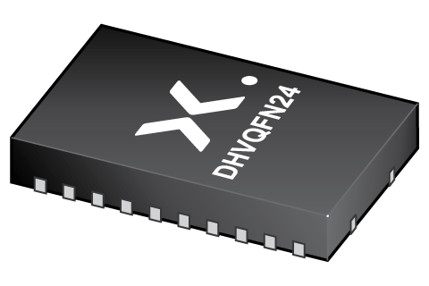
DHVQFN24 (SOT815-1) |
SOT815-1 | SOT815-1_118 | |
| 74LVC8T245PW-Q100 | 74LVC8T245PW-Q100J (935300465118) |
Active | LVC8T245 |
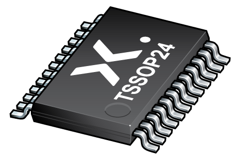
TSSOP24 (SOT355-1) |
SOT355-1 |
SSOP-TSSOP-VSO-WAVE
|
SOT355-1_118 |
| 74LVCH8T245BQ-Q100 | 74LVCH8T245BQ-Q10J (935301103118) |
Active | VCH8T245 |
DHVQFN24 (SOT815-1) |
SOT815-1 | SOT815-1_118 | |
| 74LVCH8T245PW-Q100 | 74LVCH8T245PW-Q10J (935301102118) |
Active | LVCH8T245 |
TSSOP24 (SOT355-1) |
SOT355-1 |
SSOP-TSSOP-VSO-WAVE
|
SOT355-1_118 |
環境信息
| 型號 | 可訂購的器件編號 | 化學成分 | RoHS | RHF指示符 |
|---|---|---|---|---|
| 74LVC8T245BQ-Q100 | 74LVC8T245BQ-Q100J | 74LVC8T245BQ-Q100 |
|
|
| 74LVC8T245PW-Q100 | 74LVC8T245PW-Q100J | 74LVC8T245PW-Q100 |
|
|
| 74LVCH8T245BQ-Q100 | 74LVCH8T245BQ-Q10J | 74LVCH8T245BQ-Q100 |
|
|
| 74LVCH8T245PW-Q100 | 74LVCH8T245PW-Q10J | 74LVCH8T245PW-Q100 |
|
|
文檔 (11)
| 文件名稱 | 標題 | 類型 | 日期 |
|---|---|---|---|
| 74LVC_LVCH8T245_Q100 | 8-bit dual supply translating transceiver; 3-state | Data sheet | 2023-08-10 |
| AN90063 | Questions about package outline drawings | Application note | 2025-06-13 |
| SOT815-1 | 3D model for products with SOT815-1 package | Design support | 2019-10-03 |
| SOT355-1 | 3D model for products with SOT355-1 package | Design support | 2020-01-22 |
| lvc8t245 | 74LVC8T245 IBIS model | IBIS model | 2021-02-02 |
| lvch8t245 | 74LVCH8T245 IBIS model | IBIS model | 2020-11-24 |
| Nexperia_package_poster | Nexperia package poster | Leaflet | 2020-05-15 |
| DHVQFN24_SOT815-1_mk | plastic, dual in-line compatible thermal enhanced very thin quad flat package; 24 terminals; 0.5 mm pitch; 3.5 mm x 5.5 mm x 0.85 mm body | Marcom graphics | 2017-01-28 |
| SOT815-1 | plastic, leadless dual in-line compatible thermal enhanced very thin quad flat package; 24 terminals; 0.5 mm pitch; 5.5 mm x 3.5 mm x 1 mm body | Package information | 2021-08-17 |
| SOT355-1 | plastic, thin shrink small outline package; 24 leads; 0.65 mm pitch; 7.8 mm x 4.4 mm x 1.2 mm body | Package information | 2024-11-15 |
| SSOP-TSSOP-VSO-WAVE | Footprint for wave soldering | Wave soldering | 2009-10-08 |
支持
如果您需要設計/技術支持,請告知我們并填寫 應答表 我們會盡快回復您。
Ordering, pricing & availability
樣品
作為 Nexperia 的客戶,您可以通過我們的銷售機構訂購樣品。
如果您沒有 Nexperia 的直接賬戶,我們的全球和地區分銷商網絡可為您提供 Nexperia 樣品支持。查看官方經銷商列表。