
74AUP1T34-Q100
Low-power dual supply translating buffer
The 74AUP1T34-Q100 is a single dual supply translating buffer. Input A is referenced to VCC(A) and output Y is referenced to VCC(Y). Schmitt-trigger action at all inputs makes the circuit tolerant of slower input rise and fall times. This device ensures very low static and dynamic power consumption across the entire VCC range from 1.1 V to 3.6 V. This device is fully specified for partial power down applications using IOFF. The IOFF circuitry disables the output, preventing the potentially damaging backflow current through the device when it is powered down.
This product has been qualified to the Automotive Electronics Council (AEC) standard Q100 (Grade 1) and is suitable for use in automotive applications.
Features and benefits
Automotive product qualification in accordance with AEC-Q100 (Grade 1)
Specified from -40 °C to +85 °C and -40 °C to +125 °C
Wide supply voltage range from 1.1 V to 3.6 V
CMOS low power dissipation
High noise immunity
Complies with JEDEC standards:
JESD8-7 (1.2 V to 1.95 V)
JESD8-5 (1.8 V to 2.7 V)
JESD8-B (2.7 V to 3.6 V)
Wide supply voltage range:
VCC(A): 1.1 V to 3.6 V
VCC(Y): 1.1 V to 3.6 V
Low static power consumption; ICC = 0.9 μA (maximum)
Each port operates over the full 1.1 V to 3.6 V power supply range
Latch-up performance exceeds 100 mA per JESD 78 Class II Level B
Overvoltage tolerant inputs to 3.6 V
Low noise overshoot and undershoot < 10 % of VCC
IOFF circuitry provides partial Power-down mode operation
ESD protection:
HBM: ANSI/ESDA/JEDEC JS-001 class 3A exceeds 5000 V
CDM: ANSI/ESDA/JEDEC JS-002 class C3 exceeds 1000 V
參數(shù)類(lèi)型
| 型號(hào) | VCC (V) | Logic switching levels | Output drive capability (mA) | fmax (MHz) | Nr of bits | Power dissipation considerations | Tamb (°C) | Rth(j-a) (K/W) | Ψth(j-top) (K/W) | Rth(j-c) (K/W) | Package name |
|---|---|---|---|---|---|---|---|---|---|---|---|
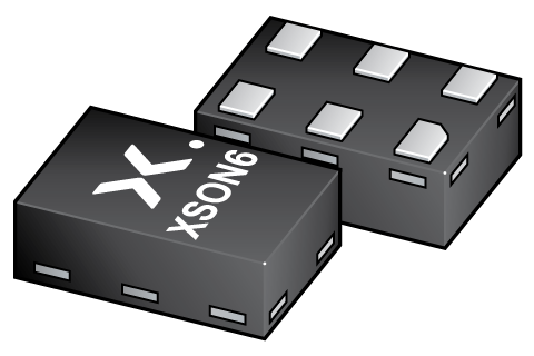
| 74AUP1T34GM-Q100 | n.a. | CMOS | ± 4 | 70 | 1 | ultra low | -40~125 | 323 | 8.4 | 164 | XSON6 |
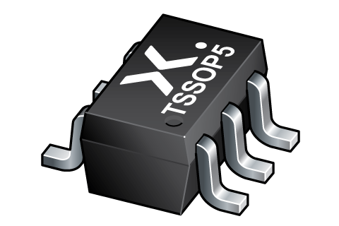
| 74AUP1T34GW-Q100 | n.a. | CMOS | ± 4 | 1 | ultra low | -40~125 | 292 | 65.6 | 165 | TSSOP5 | |
| 74AUP1T34GZ-Q100 | n.a. | CMOS | ultra low | -40~125 | 319 | 34.7 | 201.7 | XSON5 |
封裝
| 型號(hào) | 可訂購(gòu)的器件編號(hào),(訂購(gòu)碼(12NC)) | 狀態(tài) | 標(biāo)示 | 封裝 | 外形圖 | 回流焊/波峰焊 | 包裝 |
|---|---|---|---|---|---|---|---|
| 74AUP1T34GM-Q100 | 74AUP1T34GM-Q100X (935690766115) |
Active | pQ |
XSON6 (SOT886) |
SOT886 |
REFLOW_BG-BD-1
|
SOT886_115 |
| 74AUP1T34GW-Q100 | 74AUP1T34GW-Q100H (935302098125) |
Active | pQ |
TSSOP5 (SOT353-1) |
SOT353-1 |
WAVE_BG-BD-1
|
SOT353-1_125 |
| 74AUP1T34GZ-Q100 | 74AUP1T34GZ-Q100YL (935691699315) |
Active | pQ |

XSON5 (SOT8065-1) |
SOT8065-1 | SOT8065-1_315 |
環(huán)境信息
| 型號(hào) | 可訂購(gòu)的器件編號(hào) | 化學(xué)成分 | RoHS | RHF指示符 |
|---|---|---|---|---|
| 74AUP1T34GM-Q100 | 74AUP1T34GM-Q100X | 74AUP1T34GM-Q100 |
|
|
| 74AUP1T34GW-Q100 | 74AUP1T34GW-Q100H | 74AUP1T34GW-Q100 |
|
|
| 74AUP1T34GZ-Q100 | 74AUP1T34GZ-Q100YL | 74AUP1T34GZ-Q100 |
|
|
文檔 (20)
| 文件名稱(chēng) | 標(biāo)題 | 類(lèi)型 | 日期 |
|---|---|---|---|
| 74AUP1T34_Q100 | Low-power dual supply translating buffer | Data sheet | 2024-09-23 |
| AN90063 | Questions about package outline drawings | Application note | 2025-06-13 |
| Nexperia_document_guide_MiniLogic_MicroPak_201808 | MicroPak leadless logic portfolio guide | Brochure | 2018-09-03 |
| Nexperia_document_guide_MiniLogic_PicoGate_201901 | PicoGate leaded logic portfolio guide | Brochure | 2019-01-07 |
| SOT886 | 3D model for products with SOT886 package | Design support | 2019-10-03 |
| SOT353-1 | 3D model for products with SOT353-1 package | Design support | 2019-09-23 |
| SOT8065-1 | 3D model for products with SOT8065-1 package | Design support | 2024-11-05 |
| aup1t34 | 74AUP1T34 IBIS model | IBIS model | 2014-12-14 |
| Nexperia_document_leaflet_Logic_AUP_technology_portfolio_201904 | Nexperia_document_leaflet_Logic_AUP_technology_portfolio_201904 | Leaflet | 2019-04-12 |
| Nexperia_package_poster | Nexperia package poster | Leaflet | 2020-05-15 |
| Leaflet_SOT8065_Minilogic | Leaflet_SOT8065 Minilogic | Leaflet | 2024-11-15 |
| DFN1410-6_SOT886_mk | plastic, extremely thin small outline package; no leads; 6 terminals; 0.6 mm pitch; 1 mm x 1.45 mm x 0.5 mm body | Marcom graphics | 2017-01-28 |
| XSON6_SOT886_mk | plastic, extremely thin small outline package; no leads; 6 terminals; 0.6 mm pitch; 1 mm x 1.45 mm x 0.5 mm body | Marcom graphics | 2017-01-28 |
| TSSOP5_SOT353-1_mk | plastic, thin shrink small outline package; 5 leads; 0.65 mm pitch; 2 mm x 1.25 mm x 0.95 mm body | Marcom graphics | 2018-07-25 |
| SOT886 | plastic, leadless extremely thin small outline package; 6 terminals; 0.5 mm pitch; 1 mm x 1.45 mm x 0.5 mm body | Package information | 2022-06-01 |
| SOT353-1 | plastic thin shrink small outline package; 5 leads; body width 1.25 mm | Package information | 2022-11-15 |
| SOT8065-1 | Plastic thermal enhanced extremely thin small outline package withside-wettable flanks (SWF); no leads; 5 terminals; body 1.1 × 0.85 × 0.5mm | Package information | 2024-08-28 |
| REFLOW_BG-BD-1 | Reflow soldering profile | Reflow soldering | 2021-04-06 |
| MAR_SOT886 | MAR_SOT886 Topmark | Top marking | 2013-06-03 |
| WAVE_BG-BD-1 | Wave soldering profile | Wave soldering | 2021-09-08 |
支持
如果您需要設(shè)計(jì)/技術(shù)支持,請(qǐng)告知我們并填寫(xiě) 應(yīng)答表 我們會(huì)盡快回復(fù)您。
模型
| 文件名稱(chēng) | 標(biāo)題 | 類(lèi)型 | 日期 |
|---|---|---|---|
| SOT886 | 3D model for products with SOT886 package | Design support | 2019-10-03 |
| SOT353-1 | 3D model for products with SOT353-1 package | Design support | 2019-09-23 |
| SOT8065-1 | 3D model for products with SOT8065-1 package | Design support | 2024-11-05 |
| aup1t34 | 74AUP1T34 IBIS model | IBIS model | 2014-12-14 |
Ordering, pricing & availability
樣品
作為 Nexperia 的客戶(hù),您可以通過(guò)我們的銷(xiāo)售機(jī)構(gòu)訂購(gòu)樣品。
如果您沒(méi)有 Nexperia 的直接賬戶(hù),我們的全球和地區(qū)分銷(xiāo)商網(wǎng)絡(luò)可為您提供 Nexperia 樣品支持。查看官方經(jīng)銷(xiāo)商列表。