
74LVC8T595
Dual supply 8-bit serial-in/serial-out or parallel-out shift register; 3-state
The 74LVC8T595 is an 8?-?bit serial?-?in/serial or parallel?-?out shift register with a storage register and 3?-?state outputs. Both the shift and storage register have separate clocks. Data is shifted on the positive?-?going transitions of the SHCP input. The data in the shift register is transferred to the storage register on a positive?-?going transition of the STCP input. If both clocks are connected together, the shift register is always one clock pulse ahead of the storage register.
VCC(A) and VCC(B) can be supplied at any voltage between 1.1 V and 5.5 V making the device suitable for translating between any of the voltage nodes (1.2 V, 1.5 V, 1.8 V, 2.5 V, 3.3 V and 5.0 V). Pins MR, SHCP, STCP, OE, DS and Q7S are referenced to VCC(A) and pins Qn are referenced to VCC(B).
The device is fully specified for partial power?-?down applications using IOFF. The IOFF circuitry disables the output, preventing any damaging backflow current through the device when it is powered down. In suspend mode when VCC(A) is at GND level, the Qn outputs are in the high?-?impedance OFF?-?state.
Features and benefits
Wide supply voltage range:
VCC(A): 1.1 V to 5.5 V
VCC(B): 1.1 V to 5.5 V
High noise immunity
Suspend mode
Latch-up performance exceeds 100 mA per JESD 78 Class II
±24 mA output drive (VCC(A) = VCC(B) = 3.0 V)
Inputs accept voltages up to 5.5 V
IOFF circuitry provides partial Power-down mode operation
Complies with JEDEC standards:
JESD8-12A (1.1 V to 1.3 V)
JESD8-11A (1.4 V to 1.6 V)
JESD8-7 (1.65 V to 1.95 V)
JESD8-5 (2.3 V to 2.7 V)
JESD8C (3.0 V to 3.6 V)
JESD12-6 (4.5 V to 5.5 V)
ESD protection:
HBM: ANSI/ESDA/JEDEC JS-001 class 3A exceeds 4000 V
CDM: ANSI/ESDA/JEDEC JS-002 class C3 exceeds 1000 V
Specified from -40 °C to +85 °C and -40 °C to +125 °C
參數類型
| 型號 | VCC(A) (V) | VCC(B) (V) | Logic switching levels | Output drive capability (mA) | tpd (ns) | Nr of bits | Power dissipation considerations | Tamb (°C) | Rth(j-a) (K/W) | Ψth(j-top) (K/W) | Rth(j-c) (K/W) | Package name | Category |
|---|---|---|---|---|---|---|---|---|---|---|---|---|---|
| 74LVC8T595BQ | 1.1?-?5.5 | 1.1?-?5.5 | CMOS/LVTTL | ± 24 | 4.1 | 8 | low | -40~125 | 76 | 7.3 | 47 | DHVQFN20 | Uni-directional |
| 74LVC8T595PW | 1.1?-?5.5 | 1.1?-?5.5 | CMOS/LVTTL | ± 24 | 4.1 | 8 | low | -40~125 | 100 | 4.3 | 43 | TSSOP20 | Uni-directional |
封裝
| 型號 | 可訂購的器件編號,(訂購碼(12NC)) | 狀態 | 標示 | 封裝 | 外形圖 | 回流焊/波峰焊 | 包裝 |
|---|---|---|---|---|---|---|---|
| 74LVC8T595BQ | 74LVC8T595BQX (935309143115) |
Active | LVC8T595 |
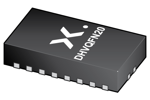
DHVQFN20 (SOT764-1) |
SOT764-1 | SOT764-1_115 | |
| 74LVC8T595PW | 74LVC8T595PWJ (935309144118) |
Active | VC8T595 |
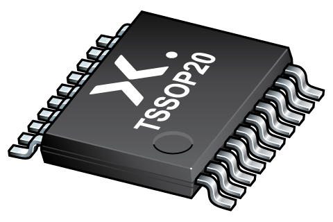
TSSOP20 (SOT360-1) |
SOT360-1 |
SSOP-TSSOP-VSO-WAVE
|
SOT360-1_118 |
環境信息
| 型號 | 可訂購的器件編號 | 化學成分 | RoHS | RHF指示符 |
|---|---|---|---|---|
| 74LVC8T595BQ | 74LVC8T595BQX | 74LVC8T595BQ |
|
|
| 74LVC8T595PW | 74LVC8T595PWJ | 74LVC8T595PW |
|
|
文檔 (12)
| 文件名稱 | 標題 | 類型 | 日期 |
|---|---|---|---|
| 74LVC8T595 | Dual supply 8-bit serial-in/serial-out or parallel-out shift register; 3-state | Data sheet | 2023-08-29 |
| AN90063 | Questions about package outline drawings | Application note | 2025-06-13 |
| Nexperia_document_guide_Logic_translators | Nexperia Logic Translators | Brochure | 2021-04-12 |
| SOT764-1 | 3D model for products with SOT764-1 package | Design support | 2019-10-03 |
| SOT360-1 | 3D model for products with SOT360-1 package | Design support | 2020-01-22 |
| Nexperia_document_leaflet_Logic_74LVC8T595_201711 | Voltage-translating Shift Register for Modular Designs | Leaflet | 2017-11-29 |
| Nexperia_package_poster | Nexperia package poster | Leaflet | 2020-05-15 |
| DHVQFN20_SOT764-1_mk | plastic, dual in-line compatible thermal enhanced very thin quad flat package; 20 terminals; 0.5 mm pitch; 2.5 mm x 4.5 mm x 0.85 mm body | Marcom graphics | 2017-01-28 |
| TSSOP20_SOT360-1_mk | plastic, thin shrink small outline package; 20 leads; 0.65 mm pitch; 6.5 mm x 4.4 mm x 1.1 mm body | Marcom graphics | 2017-01-28 |
| SOT764-1 | plastic, leadless dual in-line compatible thermal enhanced very thin quad flat package; 20 terminals; 0.5 mm pitch; 4.5 mm x 2.5 mm x 1 mm body | Package information | 2022-06-21 |
| SOT360-1 | plastic, thin shrink small outline package; 20 leads; 0.65 mm pitch; 6.5 mm x 4.4 mm x 1.2 mm body | Package information | 2024-11-15 |
| SSOP-TSSOP-VSO-WAVE | Footprint for wave soldering | Wave soldering | 2009-10-08 |
支持
如果您需要設計/技術支持,請告知我們并填寫 應答表 我們會盡快回復您。
Ordering, pricing & availability
樣品
作為 Nexperia 的客戶,您可以通過我們的銷售機構訂購樣品。
如果您沒有 Nexperia 的直接賬戶,我們的全球和地區分銷商網絡可為您提供 Nexperia 樣品支持。查看官方經銷商列表。