
74LV4094
8-stage shift-and-store bus register
The 74LV4094 is an 8?-?bit serial?-?in/serial or parallel?-?out shift register with a storage register and 3?-?state outputs. Both the shift and storage register have separate clocks. The device features a serial input (D) and two serial outputs (QS1 and QS2) to enable cascading. Data is shifted on the LOW?-?to?-?HIGH transitions of the CP input. Data is available at QS1 on the LOW?-?to?-?HIGH transitions of the CP input to allow cascading when clock edges are fast. The same data is available at QS2 on the next HIGH?-?to?-?LOW transition of the CP input to allow cascading when clock edges are slow. The data in the shift register is transferred to the storage register when the STR input is HIGH. Data in the storage register appears at the outputs whenever the output enable input (OE) is HIGH. A LOW on OE causes the outputs to assume a high?-?impedance OFF?-?state. Operation of the OE input does not affect the state of the registers. Inputs include clamp diodes. This enables the use of current limiting resistors to interface inputs to voltages in excess VCC.
Features and benefits
Optimized for low voltage applications over a wide supply voltage range from 1.0 V to 3.6 V
Accepts TTL input levels between VCC = 2.7 V and VCC = 3.6 V
Typical output ground bounce < 0.8 V at VCC = 3.3 V and Tamb = 25 °C
Typical HIGH-level output voltage (VOH) undershoot: > 2 V at VCC = 3.3 V and Tamb = 25 °C
CMOS low power dissipation
Direct interface with TTL levels
Latch-up performance exceeds 100 mA per JESD 78 Class II Level B
Complies with JEDEC standards
JESD8-7 (1.65 V to 1.95 V)
JESD8-5 (2.3 V to 2.7 V)
JESD8C (2.7 V to 3.6 V)
ESD protection:
-
HBM: ANSI/ESDA/JEDEC JS-001 class 2 exceeds 2000 V
CDM: ANSI/ESDA/JEDEC JS-002 class C3 exceeds 1000 V
Specified from -40 °C to +85 °C and from -40 °C to +125 °C
Applications
Serial-to-parallel data conversion
Remote control holding register
參數類型
| 型號 | VCC (V) | Logic switching levels | Output drive capability (mA) | tpd (ns) | fmax (MHz) | Nr of bits | Power dissipation considerations | Tamb (°C) | Rth(j-a) (K/W) | Ψth(j-top) (K/W) | Rth(j-c) (K/W) | Package name |
|---|---|---|---|---|---|---|---|---|---|---|---|---|
| 74LV4094D | 1.0?-?3.6 | TTL | ± 6 | 14 | 95 | 8 | low | -40~125 | 81 | 4.9 | 40.3 | SO16 |
| 74LV4094PW | 1.0?-?3.6 | TTL | ± 6 | 14 | 95 | 8 | low | -40~125 | 115 | 2.4 | 44 | TSSOP16 |
封裝
| 型號 | 可訂購的器件編號,(訂購碼(12NC)) | 狀態 | 標示 | 封裝 | 外形圖 | 回流焊/波峰焊 | 包裝 |
|---|---|---|---|---|---|---|---|
| 74LV4094D | 74LV4094D,118 (935088040118) |
Active | 74LV4094D |
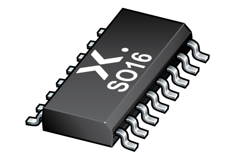
SO16 (SOT109-1) |
SOT109-1 |
SO-SOJ-REFLOW
SO-SOJ-WAVE WAVE_BG-BD-1 |
SOT109-1_118 |
| 74LV4094PW | 74LV4094PW,118 (935175020118) |
Active | LV4094 |
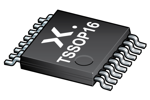
TSSOP16 (SOT403-1) |
SOT403-1 |
SSOP-TSSOP-VSO-WAVE
|
SOT403-1_118 |
下表中的所有產品型號均已停產 。
| 型號 | 可訂購的器件編號,(訂購碼(12NC)) | 狀態 | 標示 | 封裝 | 外形圖 | 回流焊/波峰焊 | 包裝 |
|---|---|---|---|---|---|---|---|
| 74LV4094DB | 74LV4094DB,112 (935166090112) |
Obsolete | no package information | ||||
| 74LV4094DB,118 (935166090118) |
Obsolete | ||||||
| 74LV4094PW | 74LV4094PW,112 (935175020112) |
Withdrawn / End-of-life | LV4094 |
TSSOP16 (SOT403-1) |
SOT403-1 |
SSOP-TSSOP-VSO-WAVE
|
暫無信息 |
環境信息
| 型號 | 可訂購的器件編號 | 化學成分 | RoHS | RHF指示符 |
|---|---|---|---|---|
| 74LV4094D | 74LV4094D,118 | 74LV4094D |
|
|
| 74LV4094PW | 74LV4094PW,118 | 74LV4094PW |
|
|
下表中的所有產品型號均已停產 。
| 型號 | 可訂購的器件編號 | 化學成分 | RoHS | RHF指示符 |
|---|---|---|---|---|
| 74LV4094DB | 74LV4094DB,112 | 74LV4094DB |
|
|
| 74LV4094DB | 74LV4094DB,118 | 74LV4094DB |
|
|
| 74LV4094PW | 74LV4094PW,112 | 74LV4094PW |
|
|
文檔 (14)
| 文件名稱 | 標題 | 類型 | 日期 |
|---|---|---|---|
| 74LV4094 | 8-stage shift-and-store bus register | Data sheet | 2024-05-28 |
| AN90063 | Questions about package outline drawings | Application note | 2025-06-13 |
| 001aaf118 | Block diagram: 74LV4094D, 74LV4094DB, 74LV4094N, 74LV4094PW | Block diagram | 2009-11-04 |
| SOT109-1 | 3D model for products with SOT109-1 package | Design support | 2020-01-22 |
| SOT403-1 | 3D model for products with SOT403-1 package | Design support | 2020-01-22 |
| Nexperia_package_poster | Nexperia package poster | Leaflet | 2020-05-15 |
| SO16_SOT109-1_mk | plastic, small outline package; 16 leads; 1.27 mm pitch; 9.9 mm x 3.9 mm x 1.35 mm body | Marcom graphics | 2017-01-28 |
| TSSOP16_SOT403-1_mk | plastic, thin shrink small outline package; 16 leads; 0.65 mm pitch; 5 mm x 4.4 mm x 1.1 mm body | Marcom graphics | 2017-01-28 |
| SOT109-1 | plastic, small outline package; 16 leads; 1.27 mm pitch; 9.9 mm x 3.9 mm x 1.75 mm body | Package information | 2023-11-07 |
| SOT403-1 | plastic, thin shrink small outline package; 16 leads; 5 mm x 4.4 mm x 1.2 mm body | Package information | 2023-11-08 |
| SO-SOJ-REFLOW | Footprint for reflow soldering | Reflow soldering | 2009-10-08 |
| SO-SOJ-WAVE | Footprint for wave soldering | Wave soldering | 2009-10-08 |
| WAVE_BG-BD-1 | Wave soldering profile | Wave soldering | 2021-09-08 |
| SSOP-TSSOP-VSO-WAVE | Footprint for wave soldering | Wave soldering | 2009-10-08 |
支持
如果您需要設計/技術支持,請告知我們并填寫 應答表 我們會盡快回復您。
Ordering, pricing & availability
樣品
作為 Nexperia 的客戶,您可以通過我們的銷售機構訂購樣品。
如果您沒有 Nexperia 的直接賬戶,我們的全球和地區分銷商網絡可為您提供 Nexperia 樣品支持。查看官方經銷商列表。