
74HCT9046A
PLL with band gap controlled VCO
The 74HCT9046A. This device features reduced input threshold levels to allow interfacing to TTL logic levels. Inputs also include clamp diodes, this enables the use of current limiting resistors to interface inputs to voltages in excess of VCC.
Features and benefits
Operation power supply voltage range from 4.5 V to 5.5 V
Low power consumption
Complies with JEDEC standard no. 7A
Inhibit control for ON/OFF keying and for low standby power consumption
Center frequency up to 17 MHz (typical) at VCC = 5.5 V
Choice of two phase comparators:
PC1: EXCLUSIVE-OR
PC2: Edge-triggered JK flip-flop
No dead zone of PC2
Charge pump output on PC2, whose current is set by an external resistor Rbias
Center frequency tolerance ±10 %
Excellent Voltage Controlled Oscillator (VCO) linearity
Low frequency drift with supply voltage and temperature variations
On-chip band gap reference
Glitch free operation of VCO, even at very low frequencies
Zero voltage offset due to operational amplifier buffering
ESD protection:
HBM JESD22-A114F exceeds 2000 V
MM JESD22-A115-A exceeds 200 V
Applications
FM modulation and demodulation where a small center frequency tolerance is essential
Frequency synthesis and multiplication where a low jitter is required (e.g. video picture?-?in?-?picture)
Frequency discrimination
Tone decoding
Data synchronization and conditioning
Voltage-to-frequency conversion
Motor-speed control
參數(shù)類型
| 型號(hào) |
|---|
封裝
下表中的所有產(chǎn)品型號(hào)均已停產(chǎn) 。
| 型號(hào) | 可訂購(gòu)的器件編號(hào),(訂購(gòu)碼(12NC)) | 狀態(tài) | 標(biāo)示 | 封裝 | 外形圖 | 回流焊/波峰焊 | 包裝 |
|---|---|---|---|---|---|---|---|
| 74HCT9046AD | 74HCT9046AD,112 (935044180112) |
Obsolete | 74HCT9046AD 74HCT9046AD Standard Procedure Standard Procedure |
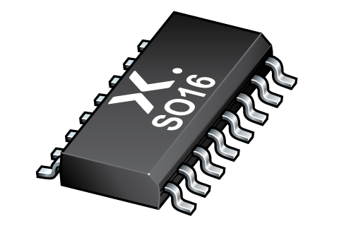
SO16 (SOT109-1) |
SOT109-1 |
SO-SOJ-REFLOW
SO-SOJ-WAVE WAVE_BG-BD-1 |
SOT109-1_112 |
| 74HCT9046AD,118 (935044180118) |
Obsolete | 74HCT9046AD 74HCT9046AD Standard Procedure Standard Procedure | SOT109-1_118 | ||||
| 74HCT9046AD,699 (935044180699) |
Obsolete | 74HCT9046AD 74HCT9046AD Standard Procedure Standard Procedure | 暫無(wú)信息 | ||||
| 74HCT9046APW | 74HCT9046APW,112 (935221200112) |
Obsolete | HT9046A Standard Procedure Standard Procedure |
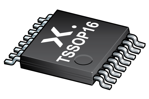
TSSOP16 (SOT403-1) |
SOT403-1 |
SSOP-TSSOP-VSO-WAVE
|
暫無(wú)信息 |
| 74HCT9046APW,118 (935221200118) |
Obsolete | HT9046A Standard Procedure Standard Procedure | SOT403-1_118 |
環(huán)境信息
下表中的所有產(chǎn)品型號(hào)均已停產(chǎn) 。
| 型號(hào) | 可訂購(gòu)的器件編號(hào) | 化學(xué)成分 | RoHS | RHF指示符 |
|---|---|---|---|---|
| 74HCT9046AD | 74HCT9046AD,112 | 74HCT9046AD |
|
|
| 74HCT9046AD | 74HCT9046AD,118 | 74HCT9046AD |
|
|
| 74HCT9046AD | 74HCT9046AD,699 | 74HCT9046AD |
|
|
| 74HCT9046APW | 74HCT9046APW,112 | 74HCT9046APW |
|
|
| 74HCT9046APW | 74HCT9046APW,118 | 74HCT9046APW |
|
|
文檔 (16)
| 文件名稱 | 標(biāo)題 | 類型 | 日期 |
|---|---|---|---|
| 74HCT9046A | PLL with band gap controlled VCO | Data sheet | 2020-03-20 |
| AN11044 | Pin FMEA 74HC/74HCT family | Application note | 2019-01-09 |
| AN90063 | Questions about package outline drawings | Application note | 2025-06-13 |
| mbd040 | Block diagram: 74HCT9046AD, 74HCT9046AN, 74HCT9046APW | Block diagram | 2009-11-03 |
| SOT109-1 | 3D model for products with SOT109-1 package | Design support | 2020-01-22 |
| SOT403-1 | 3D model for products with SOT403-1 package | Design support | 2020-01-22 |
| Nexperia_package_poster | Nexperia package poster | Leaflet | 2020-05-15 |
| SO16_SOT109-1_mk | plastic, small outline package; 16 leads; 1.27 mm pitch; 9.9 mm x 3.9 mm x 1.35 mm body | Marcom graphics | 2017-01-28 |
| TSSOP16_SOT403-1_mk | plastic, thin shrink small outline package; 16 leads; 0.65 mm pitch; 5 mm x 4.4 mm x 1.1 mm body | Marcom graphics | 2017-01-28 |
| SOT109-1 | plastic, small outline package; 16 leads; 1.27 mm pitch; 9.9 mm x 3.9 mm x 1.75 mm body | Package information | 2023-11-07 |
| SOT403-1 | plastic, thin shrink small outline package; 16 leads; 5 mm x 4.4 mm x 1.2 mm body | Package information | 2023-11-08 |
| SO-SOJ-REFLOW | Footprint for reflow soldering | Reflow soldering | 2009-10-08 |
| HCT_USER_GUIDE | HC/T User Guide | User manual | 1997-10-31 |
| SO-SOJ-WAVE | Footprint for wave soldering | Wave soldering | 2009-10-08 |
| WAVE_BG-BD-1 | Wave soldering profile | Wave soldering | 2021-09-08 |
| SSOP-TSSOP-VSO-WAVE | Footprint for wave soldering | Wave soldering | 2009-10-08 |
支持
如果您需要設(shè)計(jì)/技術(shù)支持,請(qǐng)告知我們并填寫 應(yīng)答表 我們會(huì)盡快回復(fù)您。
Ordering, pricing & availability
樣品
作為 Nexperia 的客戶,您可以通過(guò)我們的銷售機(jī)構(gòu)訂購(gòu)樣品。
如果您沒(méi)有 Nexperia 的直接賬戶,我們的全球和地區(qū)分銷商網(wǎng)絡(luò)可為您提供 Nexperia 樣品支持。查看官方經(jīng)銷商列表。